
Automatic Design Environment for Componentization of an FPGA Processing in ROS
An autonomous mobile robot which behaves according to its environment requires high performance information processing. However, it is difficult for sequential software processing to satisfy the performance requirement due to battery operation. We focus on FPGA which can realize optimized parallel processing at low power. On the other hand, FPGA can’t be employed in robot development projects since the development of an optimized circuit on FPGA is difficult and time consuming. So, we have proposed 'ROS-compliant FPGA component' for an easy integration of FPGA into any robot system. Here, we propose an automatic design environment named cReComp for componentization of FPGA processing in ROS. An experimental result shows that a software developer without any experience in FPGA can implement ROS-compliant FPGA component within one hour.
Problem in the conventional development
Figure 1 shows a conventional development flow of components in a HW/SW cooperative system design. When it comes to componentization of FPGA processing, firstly, any processing object shall be decided to be componentized. Here, we pick up User Logic as an object. For input/output data into User Logic, an interface, where a processor and FPGA can communicate each other, needs to be created. In order to create the interface, we shall design channels for data delivery in FPGA, consider communication transaction and mount circuits on FPGA. For software, we shall consider how many times write/read of data communication to the channel occur and byte counts. After the interface is created and FPGA process is componentized, one ROS-compliant FPGA component is completed when a declaration of compliance with ROS communication model is added. Since this is a development on a FPGA, to develop a User Logic, debugging for HW/SW communication and performance check shall be done. That means, that introduction of User Logic into a system causes huge development costs and it is still not efficient.
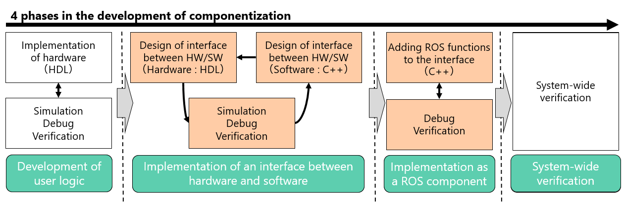
Figure 1 a flow of conventional component development in HW/SW cooperative system
Proposal of cReComp = automatic design environment for componentization
We address the above mentioned issues and propose an automatic design environment for componentization, named cReComp (creator for Reconfigurable Component) in order to improve efficiency in component development. The proposed design environment is available as Open Source at GitHub [1]. User Logic and communication transaction between SW/HW (read/write counter, size of data) shall be defined differently in each component. Then, FPGA process can be componentized automatically according to its User Logic.
System generation model for cReComp
Figure 2 shows a model generation system for cReComp. In automatic componentization of cReComp, a Scrp (Specifier for cReComp) file is used as INPUT. Scrp defines User Logic and communication transaction, which are objects to be componentized. A developer only needs to write User Logic (HDL description file) and Scrp file. He doesn’t have to write circuits description for the channel between HW/SW or software description, which are normally necessary for componentization. Corresponding to Input files, there are two kinds to be created automatically. One is Hardware (HDL description file), where control logic for the communication between HW/SW is written. The other is Software (C++ file) for accessing to FIFO buffers. These two kinds are the general terms for Interface, which is created by componentization.
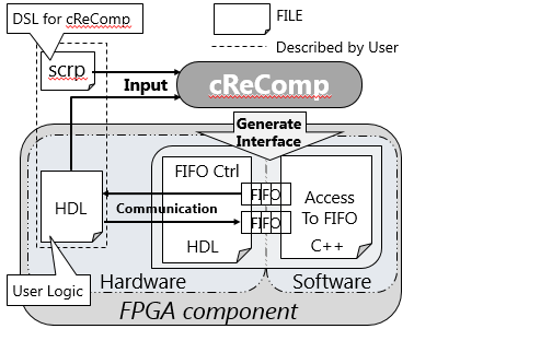
Figure 2 System generation model
Communication method of ARM-FPGA
In order to mount ‘ROS-compliant FPGA component’ to Programmable SoC (ARM+FPGA), you will need a communication channel between User Logic on FPGA and Software on a processor. To examine communication method of ARM-FPGA closely, we use Xillinux (prototype), which is a development platform for Zynq of Programmable SoC (available from Xillybus for free). Xillinux is Linux OS (Ubuntu) and operates on ARM of Zynq. It can read/write (figure 3) as a device file against FIFO buffer, which enables the communication between FPGA and ARM processor. Therefore, it connects User Logic to FIFO buffers and carries out any communication. There are 2 kinds of FIFO buffers, 32bit and 8bit. For data transfer, 32bits is used, for debugging, 8bits is used. In ‘ROS-compliant FPGA component’, there are FIFO buffers for both Input and Output to FPGA circuits. Each FIFOS is used with 32bits and also 8bits, so that ARM processers and FPGA operate independently, and Read/Write can be done at any time.
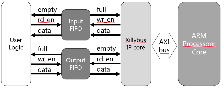
Figure 3 SW/HW communication on Xillinux
Users Logic Model as an object to be componentized and Generation of a state machine
Figure 4 shows a User Logic Model as an object to be componentized in cReComp. If the User Logic’s input signal is combinatorics, and output is register output, it can be chosen as an object. So, in order to enable the User Logic to exchange data with the processor, cReComp generates a state machine as shown in Figure 5. When the processor inputs data to User Logic, it receives data from a FIFO buffer of Input in a READY_RCV state and a RCV_DATA state, then outputs data to the User Logic. When the User Logic outputs data to the processor, it outputs values of the register output of the User Logic to a FIFO buffer of Output directly. As of today, the User Logic is directly created by HDL description, however, in near future it will be applicable for various formats.
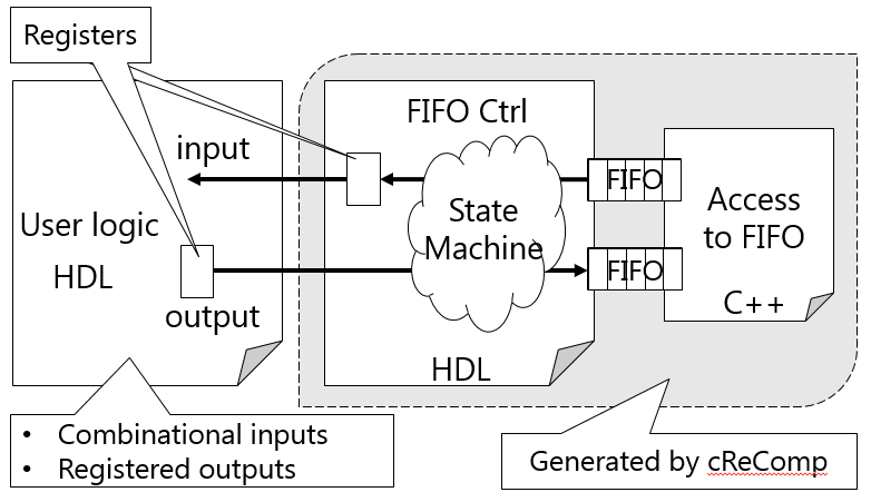
Figure 4, a User Logic Model as an object to be componentized
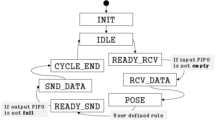
Figure 5, a state machine to control FIFO buffers
Definition of SW/HW communication transaction by Scrp file
In cReComp, a communication transaction between software and hardware is defined by a Scrp file. An example of Scrp file is shown in Figure 6. A template can be generated by using cReComp. Each setting item is called FLAG. By defining according to each FLAG, components can be automatically generated. The FLAG in Table 1 is only for 32bit FIFO. Any FLAG with * is for both 32bit and 8bit FIFO. And also, in cReComp, if a User Logic is specified during Scrp File template generation, input/output signals for a circuit of the User Logic will be described in the template automatically. So, without writing HDL description for the circuit of SW/HW communication transaction, it is possible to wire signals in the Scrp file freely.
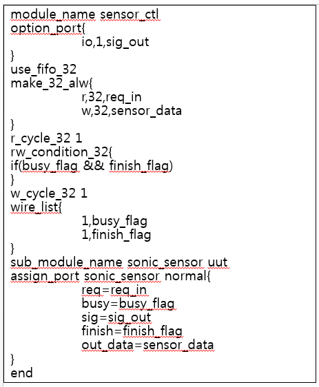
Figure6 Example of Scrp file
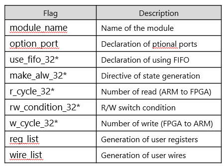
Table 1 Definition of each flug in Scrp file
[1]cReComp : https://github.com/kazuyamashi/cRecomp.git